Total Quality Control will also mean trust in quality, confidence in quality: Shri Goyal
Bureau of Indian Standards (BIS) completed 75 glorious years of its existence on 6th January 2022. BIS came into existence as the Indian Standards Institution (ISI) in 1947. Through its core activities of Standardization and Certification, BIS has been contributing to the national economy for the past 75 years.
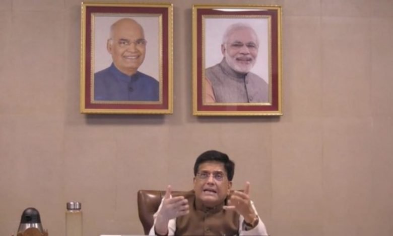
Shri Piyush Goyal, Union Minister, Ministry of Consumer Affairs, Food & Public Distribution, Commerce & Industry and Textiles congratulated the institution and all associated with it via video conferencing.

While addressing the officers of the Ministry of Consumer Affairs, Food and Public Distribution and Bureau of Indian Standards, he said, “Honourable Prime Minister before even becoming the Chief Minister of Gujarat gave the concept of 3S- Speed, Skill and Scale. It’s time now to change it to 4S – Speed, Skill, Scale and Standards.
He said that as we celebrate Azadi Ka Amrit Mahotsav, it’s a nice coincidence as well as an opportunity to reflect that in the words of Prime Minister it’s the beginning of ‘Amrit Kal of Azadi’. “Both the Nation and BIS will be completing 100 years in 2047 so it’s going to be a great opportunity for BIS to plan and chart out our 25-year agenda from now until 2047. How we will contribute to make India a world power and a superpower and a great nation,” he said.
Every single action demands quality that should be our mantra: Shri Goyal
Shri Goyal said that the defining feature that distinguishes some of the countries from us is focused on quality, “And if we can take it up as a mission that if 135 crore Indians start demanding quality and every participant in economic activity in India provides quality, then quality will speak for itself”.
He said that the Centre is working towards a One Nation One Standard. And it’s important to set the benchmark by working skilfully so that we are internationally aligned.
Shri Goyal said that the standardization and conformity assessment will also provide consumers, safe, reliable and high-quality products and therefore, our job becomes important and relevant in the years to come.
“Many manufacturing units today look at Total Quality Control or Six Sigma level of quality where they are counting defects or errors and very strict measures are taken and that is Hallmark of a progressive, modern and developed nation,” he added.
He stressed that BIS will make consumers more aware regarding quality. Total Quality Control will also mean trust in quality, confidence in quality.
Shri Goyal complemented the Bureau of Indian Standards in making Hallmarking and Assaying a success. He said, “Äs we celebrate Azadi K Amrit Mahotsav this year and plan for Amrit Kal for next 25 years, BIS also play an equally important role in building a brand India so that we get recognized the world over as a quality supplier of goods and services changing the mindset of the nation.”
Quality is not expensive it is cost effective: Shri Goyal
“Every single action demands quality that should be our mantra,” he added.
Shri Goyal also suggested 5 Mantras for BIS to grow:
“1-We should work as a facilitator, not an obstructer.
2-BIS to develop as a global organization. Learning from global experiences, integrating global standards. Show the world we are the best. For this, we have to be pioneers also.
3-Working on Gap analysis to assess laboratory attesting needs of the country and set up high-quality modern labs across India.
4-Nothing short of quality or standard revolution is required. One Nation One Standard will become a game-changer in this regard.
5-Quality is not expensive it is cost-effective, ” he said.
Shri Rohit Kumar, Secretary Department of Consumer Affairs along with Ms Nidhi Khare, Additional Secretary and other officers of the Ministry and BIS participated in the event.
Shri Pramod Kumar Tiwari, Director General of Bureau on the special occasion extended his gratitude and best wishes to all the stakeholders of BIS. He said, “It is due to the constant efforts and strive for excellence of employees and other stakeholders of BIS that we have been able to achieve this respectable place today. We commit to contribute further in future with more zeal and dedication in India’s progress”.
BIS celebrates its 75th Anniversary
In the twilight years of British rule in India, when the country was faced with the gigantic task of building up the industrial infrastructure, it was the Institution of Engineers (India), which prepared the first draft of the Constitution of an Institution that could take up the task of formulation of National Standards. This lead to the Department of Industries and Supplies issuing a memorandum on 3rd September 1946, formally announcing the setting up of an organization called the ‘Indian Standards Institution (ISI). ISI came into being on the 6th January 1947 and in June 1947 Dr Lal C. Verman took over as its first Director.
Bureau of Indian Standards (BIS) came into existence, through an Act of Parliament dated 26th November 1986, on 1st April 1987, with a broadened scope and more powers; taking over the staff, assets, liabilities and functions of erstwhile ISI. Through this changeover, the government envisaged building a climate for quality culture and consciousness and greater participation of consumers in the formulation and implementation of standards.
Disclaimer : This is an official press release by PIB.