Minister of State Rajeev Chandrasekhar reviews Gallium Nitride Technology centre – GEECI, Bengaluru
“Coming 2 to 3 years offers window of opportunity for Gallium Nitride (GaN) to play key role in enabling India’s ambition to lead Automotive and Mobility innovation” – Rajeev Chandrasekhar
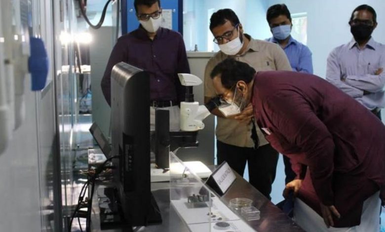
Union Minister of State for Electronics & Information Technology and Skill Development & Entrepreneurship, Rajeev Chandrasekhar visited the Gallium Nitride Ecosystem Enabling Centre and Incubator ( GEECI ) facility at the prestigious Indian Institute of Sciences (IISc), Bengaluru. The facility has been jointly set up by the Ministry of Electronics and Information Technology and IISc Bengaluru aimed at establishing a GaN-based Development Line Foundry facility, especially for RF and power applications, including strategic applications.
The Minister after reviewing the progress of the Project and after inspecting the facility highlighted its importance by stating that “The next 2 to 3 years offers a window of opportunity for Gallium Nitride (GaN) to play a key role in enabling e-vehicles and wireless communication”. Minister also saw the GaN transistors fabricated in the IISc CeNSE fab.


Creating strategic capabilities in emerging technologies is one of the core objectives of the Digital India Programme launched by Prime Minister Narendra Modi in the year 2015. To achieve these objectives, the Ministry of Electronics and IT has drawn MeiTY vision for 1000 days which includes HiTech/Strategic Tech as an important component. Gallium Nitride Technology is of strategic importance with its application to 5G, space and defence applications.
The Minister spoke about the recently experienced Covid induced disruptions in the Global Supply Chains and how the Government, led by PM Narendra Modi, is committed to capitalising on this narrow window of opportunity that is presented to India – as the world is looking for a new and trusted supply chain partner.
“Developing Global leadership in emerging technologies is one of the objectives of Digital India Programme launched by the PM Narendra Modi “ – Rajeev Chandrasekhar
“There is tremendous opportunity in the electronics manufacturing & in the field of electronics and semiconductor design”, said Mr Rajeev Chandrasekhar as he mentioned the recently announced $10 billion incentive package for setting up Semi-Conductor fab units in India and to make India a global hub for Electronics systems design and manufacturing (ESDM).
“Research, technology development, education and training in our institutes like IISc and IITs in the area of semiconductor manufacturing is essential to realise the dream of Digital India and fabs in the nation” added Mr Rajeev Chandrasekhar.
The fab model in IISc will be a state of the art incubation to promote indigenous development of technology, and thereby encourage final deployment into cellular infrastructure, and strategic technologies.
Along with PLI and DLI schemes, the GaN ecosystem will drive innovation and encourage startups and entrepreneurs to look into business and technology seriously in the next two years. AGNIT Semiconductors Pvt. Ltd. the first startup has already been incubated in TBI-InCeNSE an incubator of SID, IISc. It has raised its first round of angel funding. This will be the first startup to leverage the infrastructure created by GEECI.
Disclaimer : This is an official press release by PIB.